Just the right touch:
Producing semiconductors for energy-saving high-performance electronics

Pure silicon is extremely brittle and has a metallic luster. It is also an extremely poor conductor of electricity. To create the highly sought-after n- and p-type semiconductors that make our modern world go round, silicon needs to be doped with small amounts of “foreign” atoms such as phosphorous or boron. Modifying the surface of silicon is sufficient to create substrates for small electronic components. n-type semiconductors, for instance, are produced by bombarding silicon with phosphorus ions. Only trace amounts of phosphorus are needed to transform an entire silicon crystal into an n-type semiconductor during production. However, even the slightest variation in concentration can limit the suitability of silicon produced in this manner for high-performance electronics. Which is where neutron doping comes in.
As far back as the 1950s, scientists discovered an ideal way of creating n-type semiconductors. They observed that when a slow neutron collides with a silicon core with a mass number of 30, unstable silicon-31 is created. With a half-life of two-and-a-half hours, these atoms quickly decay into phosphorus-31. This nuclear reaction proved ideal for n-type semiconductors for two very good reasons. Firstly, natural silicon comprises around three-percent silicon-30. Secondly, the resulting phosphorus is not radioactive. In other words, the “doped” silicon can be implemented in all manner of applications. Furthermore, the dopant atoms of semiconductor material created in this way are extremely evenly distributed. The crystal structure also contains very few defects. All of which makes it ideal for high-performance components. The TU Munich’s neutron source FRM II is particularly well equipped to carry out this kind of doping as it produces hardly any fast neutrons. When a fast neutron collides with a silicon atom, the speed of the impact damages the crystal structure and greatly impairs the silicon’s ability to function as a semiconductor.
Neutron-doped silicon is primarily required for high-power thyristors and transistors commonly found in electric power systems. High-voltage DC power lines are particularly challenging due to the vast amounts of electricity they transport. Yet when it comes to long-distance power supply, they are much more efficient than AC power lines. The supply lines carrying electricity from Mozambique’s Cabora Bassa dam to South Africa or the power lines linking Tasmania to Australia are two classic examples of this. Similarly, offshore wind parks would not be viable with AC lines. High-voltage DC power lines are currently capable of transporting voltages up to +/- 500 kilovolt. The next generation will see capacity rise to +/- 800 kilovolt. Thyristors that can withstand voltages in excess of 6000 megawatts are currently being developed for this purpose.
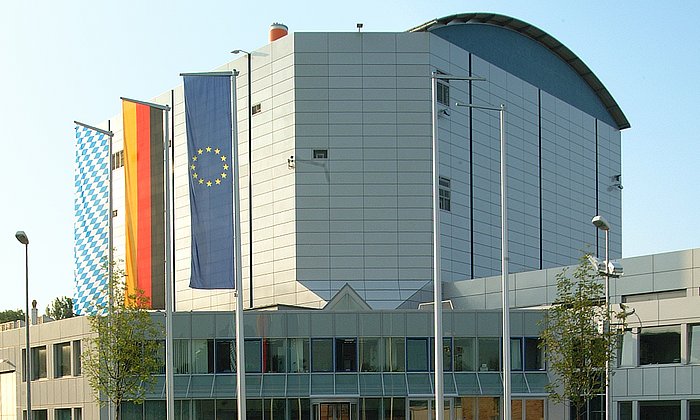
Back when the FRM II neutron source was being built, engineers designed dedicated neutron irradiation facilities offering sample test services for research and industry. The silicon doping facility is the largest of these. Silicon rods with diameters of up to 20 centimeters can be arranged in stacks of up to 50 centimeters in a cylinder one meter from the reactor’s core. To ensure homogeneous irradiation, the container holding the silicon cylinders slowly rotates on its own axis. However, even when the rods are in an upright position they are not subjected to a uniform flow of neutrons. Our scientists solved this problem by deploying a nickel cylinder that is slightly thicker at points where neutrons are highly concentrated. Much like a contact lens, this cylinder then compensates for any inequalities.
Industry interest in the FRM II irradiation facilities was great even during the development phase. And once the reactor was up and running, the first orders started rolling in. Due to increased demand, the head of irradiation services at FRM II, Dr. Heiko Gerstenberg, decided to replace the initial semi-automatic conveyor with a fully automatic loading and unloading unit in February 2007. This program-controlled unit transports the samples from the storage pool and positions them for irradiation. It then inserts the samples and removes them once irradiation is complete. This procedure has now been in use for just over a year, enabling the installation to enrich 3.8 tons of silicon in 2007. “None of our industry work has negatively impacted our research,” emphasizes Dr. Heiko Gerstenberg. And thanks to a further rise in demand, FRM II has now ramped up operations even further. From this month onwards, the installation will be operating in two shifts.
Images:
After doping the silicon cylinder is lifted from the irradiation position: Link to the picture
A cylinder of pure neutron-doped silicon is cleaned for shipment in the laboratory: Link to the picture
Contact:
Dr. Heiko Gerstenberg
Technische Universität München
Research Neutron Source Heinz Meier-Leibnitz
Irradiation Service
Lichtenbergstr. 1
D-85747 Garching
Tel.: +49 89 289 12145
Fax: +49 89 289 12191
E-Mail: heiko.gerstenberg@frm2.tum.de
Web: www.frm2.tum.de
![[Translate to en:] Reaktorbecken im FRM II. (Foto: Andreas Heddergott) [Translate to en:] Reaktorbecken im FRM II. (Foto: Andreas Heddergott)](/fileadmin/_processed_/b/1/csm_Erste-Neutronen_EH20100303501_1200x675_neu_45e5bf3c5a.jpg)


![[Translate to en:] Prof. Dr. Pfleiderer bereitet eine Probe in der Forschungs-Neutronenquelle Heinz Maier-Leibnitz vor. (Photo: Wenzel Schuermann / TUM) [Translate to en:] Prof. Dr. Pfleiderer bereitet eine Probe in der Forschungs-Neutronenquelle Heinz Maier-Leibnitz vor. (Photo: Wenzel Schuermann / TUM)](/fileadmin/_processed_/2/1/csm__DSC9919_1200x675_Neu_ab8da04b56.jpg)


